Consider the design of a logic circuit that counts
the number of 1's in a bit-serial input stream. If the circuit asserts its
output when the input stream contains an odd number of 1's, it is called
an odd parity checker. If it asserts its output when it has seen
an even number of 1's, it is an even parity checker. The circuit
is clearly sequential: the current output depends on the complete history
of inputs.
State Diagram The first step of
our design process is to develop a state diagram that describes the behavior
of the circuit. It's not too hard to see that the circuit can be in one
of two different states: either an even or an odd number of 1's has been
seen since reset. Whenever the input contains a 1, we switch to the opposite
state. For example, if an odd number of 1's has already been seen and the
current input is 1, we now see an even number of 1's. If the input is 0,
we stay in the current state.
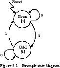
The state diagram we derive is shown in Figure 8.1.
We name the two unique configurations of the circuit Even and Odd. The outputs are explicitly associated with the states and are shown in square brackets. When an odd number of 1's has been seen, the output is 1. Otherwise it is 0. We associate the input values that cause a transition to take place with the arcs in the state diagram.
State Transition Table A reformulation of the state diagram is the symbolic state transition table. This is shown in Figure 8.2. We give meaningful -symbolic names to the inputs, outputs, and present and next states. We cannot implement the circuit just yet. We must first assign binary encodings to all the state, input, and output symbols in the transition table.
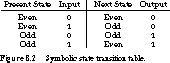
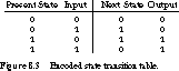
Figure 8.3 shows the revised representation, called the encoded state table. We have assigned the encoding 0 to state Even and 1 to state Odd. The table now looks more like a truth table.
Next State and Output Functions At
this point, we have the next state (NS) and output
(OUT) expressed as logic functions of the present
state (PS) and present input (PI).
Based on a quick examination of the encoded state table, we write the functions
as
Implementation Now we are ready to implement the circuit. The state of the finite state machine is held by flip-flops. Since we have only two states, we can implement the circuit with a single flip-flop. The next-state function determines the input to this flip-flop.NS =PSÝPI OUT=PS
We show an implementation using a D flip-flop
in Figure 8.4(a).
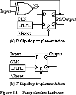
The XOR gate directly computes the D input as a function of the present state and the input.
A close inspection of the state transition table should
suggest to you an alternative implementation. Whenever the input is 0, the
circuit stays in the same state. Whenever the input is 1, the state toggles.
An implementation based on a T flip-flop is given in Figure 8.4(b).
This eliminates the XOR gate. By judicious selection of the flip-flop type,
you can simplify the implementation logic.
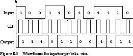
Figure 8.5 shows the abstract timing behavior of the
finite state machine for the input stream 100110101110. Each input bit is
sampled on the rising edge of the clock because the state register is implemented
by a positive edge-triggered flip-flop. The output changes soon after the
rising edge. You should be able to convince yourself that the output is
1 whenever the input stream has presented an odd number of 1's, and is 0
otherwise.
(positive
edge) or high-to-low (negative edge)
transitions on the clock. In a positive edge-triggered system, the state
time is measured from one rising clock edge to the next. In negative edge-triggered
systems, the state time is measured between subsequent falling edges.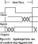
Figure 8.6 illustrates the state change, input sampling, and output changes for a positive edge-triggered synchronous system. On the rising edge, the inputs and current state are sampled to compute the new state and outputs.
Output Validity An output is
not valid until after the edge, and inputs are sampled just before the edge.
As an example of detailed state machine timing behavior, Figure 8.7 gives
fragment state diagrams for two communicating finite state machines (FSMs).
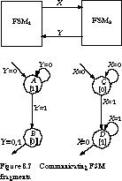
We assume that both are positive edge-triggered synchronous systems and the output from each state machine is the input to the other. The interaction between these machines is illustrated by the timing diagram of Figure 8.8.
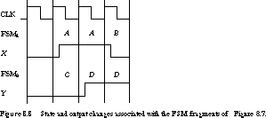
To start, the clock is in the first period with FSM1
about to enter state A with its output X =
0. FSM2 is entering state C with its output Y =
0. In the second clock period, FSM1 is in state A and asserts its
output X. FSM2 is in state C with its output Y
unasserted. On the rising edge that starts the third clock period, FSM1
stays in state A since its input is 0. FSM2 advances to state D,
asserting Y, but too late to affect the state change in FSM1. The
input value before the clock edge is the one that matters.
Now that Y is 1, FSM1 goes to state B
on the next rising edge. In this state, it will output a 0, but this is
too late to affect FSM2's state change. It remains in state D.
[Top] [Next]
[Prev]