 Recently, we have carried out PLAD of YSZ/YBCO bilayers onto NiFe (50:50) substrates. Results, which show a great sensitivity on the deposition parameters, are twofold. Form the structural point of view, a relatively good degree of epitaxial growth and in-plane biaxial texture can be achieved. On the other hand, electrical properties are still not adequate for exploitation in power transport devices.
Such a discrepancy gave us motivations for a detailed microscopic analysis of our samples, based on atomic force (AFM) and near-field optical microscopy (SNOM) and carried out in strict collaboration with the SPM group led by Prof. Maria Allegrini. Morphology of the YBCO surface layer turned out to be rather rough, probably as a consequence of substrate oxidization, and the near-field analysis revealed a non-homogeneous scattering from the surface, related to local variations of the stoichiometry at the grain, or inter-grain scale. Further analysis and interpretation for our findings are presently in progress.
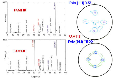
XRD patterns and pole figures of YBCO/YSZ/NiFe samples deposited by PLAD and showing that, under an appropriate choice of process parameters (FAM118), adequate degrees of epitaxial growth and biaxial texture can be achieved.
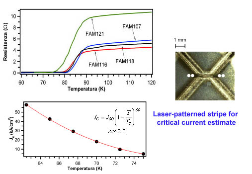
Some results of electrical characterization of YBCO/YSZ/NiFe samples deposited by PLAD. Critical current has been estimated by measuring the I-V characteristics at different temperatures on laser-patterned stripes (typically, 0.1 mm wide).
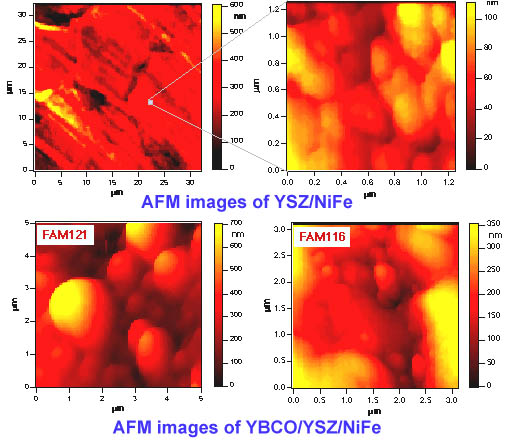
AFM images of an YSZ/NiFe sample (topp panels, with different magnification) and of YBCO/YSZ/NiFe samples, all deposited by PLAD. Low magnification analysis of the YSZ layer (grown in HV conditions) exhibits the presence of large polygonal grains related with the textured polycrystalline nature of the substrate (textured by cold rolling and annelaing). YBCO surface shows a rough morphology, which, along with the grain size, depends on the process parameters. In films with better structural and electrical properties (e.g., FAM116), grains are larger and their relative arrangement is more compact.
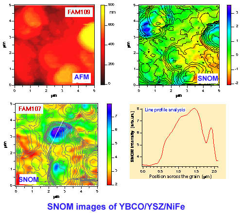
In the top panel, comparison between AFM and SNOM images of the same portion of an YBCO/YSZ/NiFe sample deposited by PLAD. Features pertaining only to the optical analysis are visible, with a sub-wavelength space resolution. In the bottom panel, SNOM image of an YBCO/YSZ/NiFe sample deposited by PLAD with superimposed the curve levels of the topography. Inhomogeneous space distribution of the optical near-field scattered intensity is observed along one large-size grain, as demonstrated by the corresponding line-profile analysis. Such gradient-like behavior is typical in samples grown with a specific choice of the deposition paramters, and can be possibly related to local fluctuations in the YBCO stoichiometry which might affect the elctrical transport properties.